- 您现在的位置:买卖IC网 > Sheet目录337 > LH28F320S3HNS-ZM (Sharp Microelectronics)IC FLASH 32MBIT 110NS 56SSOP
�� �
�
�LHF32KZM�
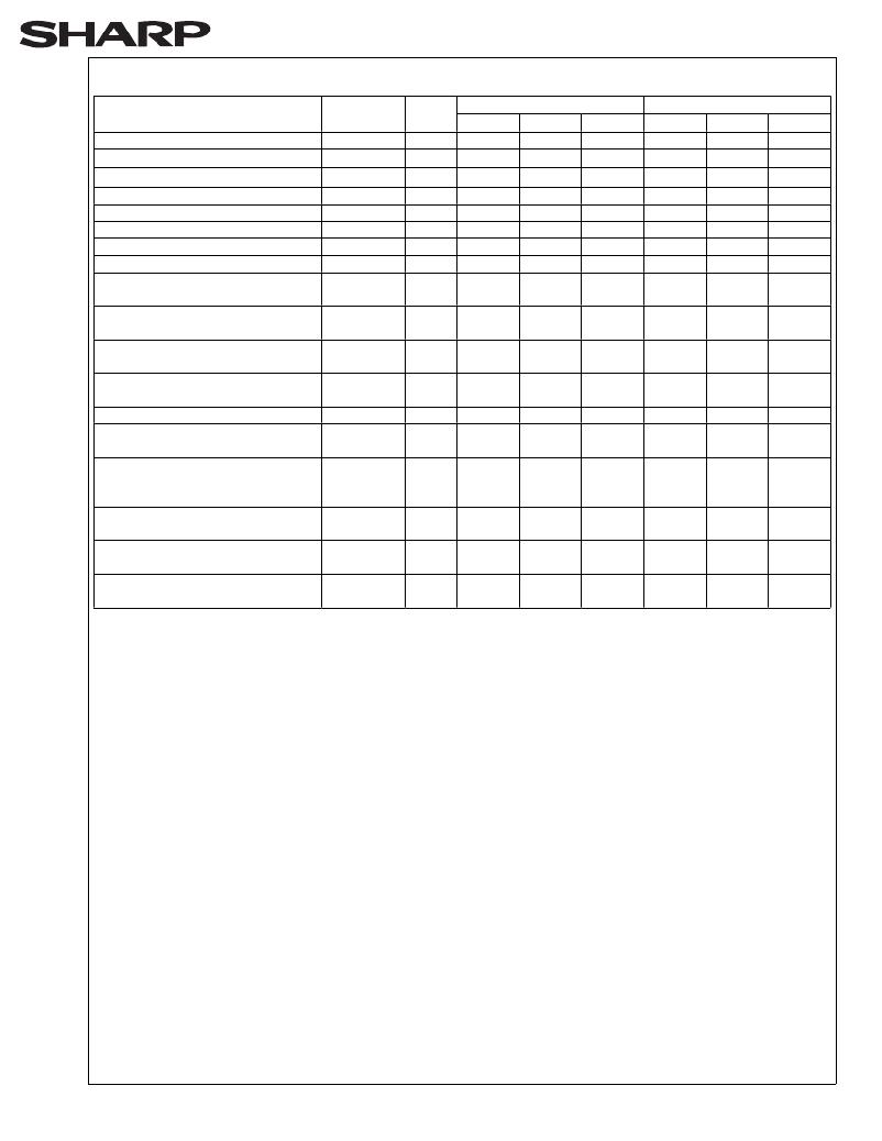
�Table� 4.� Command� Definitions� (10)�
�11�
�Bus� Cycles� Notes�
�First� Bus� Cycle�
�Second� Bus� Cycle�
�Command�
�Req’d�
�Oper� (1)�
�Addr� (2)�
�Data� (3)�
�Oper� (1)�
�Addr� (2)�
�Data� (3)�
�Read� Array/Reset�
�1�
�Write�
�X�
�FFH�
�Read� Identifier� Codes�
�Query�
�Read� Status� Register�
�≥� 2�
�≥� 2�
�2�
�4�
�Write�
�Write�
�Write�
�X�
�X�
�X�
�90H�
�98H�
�70H�
�Read�
�Read�
�Read�
�IA�
�QA�
�X�
�ID�
�QD�
�SRD�
�Clear� Status� Register�
�1�
�Write�
�X�
�50H�
�Block� Erase� Setup/Confirm�
�Full� Chip� Erase� Setup/Confirm�
�Word/Byte� Write� Setup/Write�
�Alternate� Word/Byte� Write�
�Setup/Write�
�Multi� Word/Byte� Write�
�Setup/Confirm�
�2�
�2�
�2�
�2�
�≥� 4�
�5�
�5,6�
�5,6�
�9�
�Write�
�Write�
�Write�
�Write�
�Write�
�BA�
�X�
�WA�
�WA�
�WA�
�20H�
�30H�
�40H�
�10H�
�E8H�
�Write�
�Write�
�Write�
�Write�
�Write�
�BA�
�X�
�WA�
�WA�
�WA�
�D0H�
�D0H�
�WD�
�WD�
�N-1�
�Block� Erase� and� (Multi)�
�Word/byte� Write� Suspend�
�Confirm� and� Block� Erase� and�
�(Multi)� Word/byte� Write� Resume�
�1�
�1�
�5�
�5�
�Write�
�Write�
�X�
�X�
�B0H�
�D0H�
�Block� Lock-Bit� Set� Setup/Confirm�
�Block� Lock-Bit� Reset�
�Setup/Confirm�
�2�
�2�
�7�
�8�
�Write�
�Write�
�BA�
�X�
�60H�
�60H�
�Write�
�Write�
�BA�
�X�
�01H�
�D0H�
�STS� Configuration�
�Level-Mode� for� Erase� and� Write�
�2�
�Write�
�X�
�B8H�
�Write�
�X�
�00H�
�(RY/BY#� Mode)�
�STS� Configuration�
�Pulse-Mode� for� Erase�
�STS� Configuration�
�Pulse-Mode� for� Write�
�STS� Configuration�
�Pulse-Mode� for� Erase� and� Write�
�2�
�2�
�2�
�Write�
�Write�
�Write�
�X�
�X�
�X�
�B8H�
�B8H�
�B8H�
�Write�
�Write�
�Write�
�X�
�X�
�X�
�01H�
�02H�
�03H�
�NOTES:�
�1.� BUS� operations� are� defined� in� Table� 3� and� Table� 3.1.�
�2.� X=Any� valid� address� within� the� device.�
�IA=Identifier� Code� Address:� see� Figure� 4.�
�QA=Query� Offset� Address.�
�BA=Address� within� the� block� being� erased� or� locked.�
�WA=Address� of� memory� location� to� be� written.�
�3.� SRD=Data� read� from� status� register.� See� Table� 14� for� a� description� of� the� status� register� bits.�
�WD=Data� to� be� written� at� location� WA.� Data� is� latched� on� the� rising� edge� of� WE#� or� CE#� (whichever� goes� high�
�first).�
�ID=Data� read� from� identifier� codes.�
�QD=Data� read� from� query� database.�
�4.� Following� the� Read� Identifier� Codes� command,� read� operations� access� manufacturer,� device� and� block� status�
�codes.� See� Section� 4.2� for� read� identifier� code� data.�
�5.� If� the� block� is� locked,� WP#� must� be� at� V� IH� to� enable� block� erase� or� (multi)� word/byte� write� operations.� Attempts�
�to� issue� a� block� erase� or� (multi)� word/byte� write� to� a� locked� block� while� RP#� is� V� IH� .�
�6.� Either� 40H� or� 10H� are� recognized� by� the� WSM� as� the� byte� write� setup.�
�7.� A� block� lock-bit� can� be� set� while� WP#� is� V� IH� .�
�8.� WP#� must� be� at� V� IH� to� clear� block� lock-bits.� The� clear� block� lock-bits� operation� simultaneously� clears� all� block�
�lock-bits.�
�9.� Following� the� Third� Bus� Cycle,� inputs� the� write� address� and� write� data� of� ’N’� times.� Finally,� input� the� confirm�
�command� ’D0H’.�
�10.� Commands� other� than� those� shown� above� are� reserved� by� SHARP� for� future� device� implementations� and�
�should� not� be� used.�
�Rev.� 1.6�
�发布紧急采购,3分钟左右您将得到回复。
相关PDF资料
LH28F320SKTD-ZR
IC FLASH 32MBIT 70NS 48TSOP
LHF00L28
IC FLASH 16MBIT 70NS 48TSOP
LPM409 CHASSIS
STNRD 4SLOT CHASSIS W/INPUT LEAD
LS15RB1201J04
POE SPLITTER 10.8W 12V @0.9A
LT1932ES6#TRMPBF
IC LED DRIVR WHITE BCKLGT TSOT-6
LT1937ES5#TRMPBF
IC LED DRIVR WHITE BCKLGT TSOT-5
LT3003EMSE#TRPBF
IC LED DRIVER BALLASTER 10-MSOP
LT3465AES6#TRMPBF
IC LED DRIVR WHITE BCKLGT TSOT-6
相关代理商/技术参数
LH28F320S3-L11
制造商:SHARP 制造商全称:Sharp Electrionic Components 功能描述:32-MBIT(4MBx8/2MBx16)Smart 3 Flash MEMORY
LH28F320S3-L110
制造商:SHARP 制造商全称:Sharp Electrionic Components 功能描述:32-MBIT(4MBx8/2MBx16)Smart 3 Flash MEMORY
LH28F320S3-L130
制造商:SHARP 制造商全称:Sharp Electrionic Components 功能描述:32-MBIT(4MBx8/2MBx16)Smart 3 Flash MEMORY
LH28F320S3-L14
制造商:SHARP 制造商全称:Sharp Electrionic Components 功能描述:32-MBIT(4MBx8/2MBx16)Smart 3 Flash MEMORY
LH28F320S3-L140
制造商:SHARP 制造商全称:Sharp Electrionic Components 功能描述:32-MBIT(4MBx8/2MBx16)Smart 3 Flash MEMORY
LH28F320S3-L160
制造商:SHARP 制造商全称:Sharp Electrionic Components 功能描述:32-MBIT(4MBx8/2MBx16)Smart 3 Flash MEMORY
LH28F320S3NS
制造商:SHARP 制造商全称:Sharp Electrionic Components 功能描述:Smart voltage 32Mbit Flash Memory
LH28F320S3NS-L11
功能描述:IC FLASH 32MBIT 110NS 56SSOP RoHS:否 类别:集成电路 (IC) >> 存储器 系列:- 标准包装:60 系列:- 格式 - 存储器:EEPROMs - 串行 存储器类型:EEPROM 存储容量:16K (2K x 8) 速度:2MHz 接口:SPI 3 线串行 电源电压:2.5 V ~ 5.5 V 工作温度:-40°C ~ 85°C 封装/外壳:8-DIP(0.300",7.62mm) 供应商设备封装:8-PDIP 包装:管件 产品目录页面:1449 (CN2011-ZH PDF)